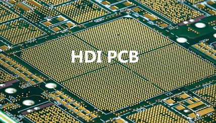
In general, HDI is defined as High-density interconnect. It is a circuit board in specific it is a printed circuit board with a higher wiring density per unit area. When compared with typically printed circuit boards, HDI PCB provided vast wiring. Furthermore, HDI PCB is one of PCBs with various features such as micro vias, blind and buried vias, built-up laminations, and high signal performance. To date, the printed circuit board is getting changed in terms of technology; that’s the reason behind smaller and faster products.
Additionally, HDI is compact with tiny vias, pads, copper traces, and spaces. HDI has denser wiring through lighter weight, more compact, lower layer PCBs formed. Henceforth, using one HDI board is enough that will give utter functionality. Also, using HDI will assist designers in placing more components on both sides of the raw PCB. You can set various smaller parts together. HDI can use on multiple devices, including mobile phones, touch-screen devices, laptop computers, digital cameras, 4G network communications.
How best is HDI?
As mentioned earlier, HDI is beneficial when compared with traditional ones. Importantly, it will let designers straightforwardly incorporate more components onto smaller boards. Even designers can set pieces on both sides of the board. Significantly, it will decrease power usage; as a result, it will enhance the battery life in handheld and other battery-powered devices.
Further, it is solid and rugged that will offer you better strength. Along with that, it will reduce thermal degradation by increasing the device’s life. That will provide better efficiency and higher density transmission and computation in smaller areas. And that’s the reason for implementing end-user products such as smartphones, aerospace equipment, military devices, and medical equipment. Also, HDI technology improves functionality that will reduce the size and weight of products.
Notably, there will be only less distance between components which will enhance electrical performance. As a result, only less power will be consumed.
How beneficial is using HDI PCB?
When it comes to heat transfer in HDI PCB, which gets decreased because the heat wants to travel only a less distance. Similarly, another feature you should notify in HDI PCB is that it will undergo thermal expansion, which will increase over time; therefore, the tension will get reduced, and it defines the long-lasting characteristics.
In general, the HDI PCB board is either a conductive or non-conductive transmitter. According to your requirements depending upon the solitary shape and size of your board, it has better proficiency. Next, the blind vias allow the constituents of the board to get placed closer to each other. When the distance between the components is reduced, and the path is direct, the signal strength grows stronger.
In short, it has reduced risk. The best way to eliminate vulnerability in the gadgets is to stop them from mechanical shocks. One important thing is that the advanced HDI carries lesser weight when compared with its counterparts.
How does it help?
Besides, HDI boards are cost-effective when compared with other options. Alongside, it requires fewer raw materials due to their smaller size and the low number of layers. Eventually, it will give functionality and value to the device.